The Global Solar Photovoltaic Supply Chain and Bottom-UP Cost Model Results
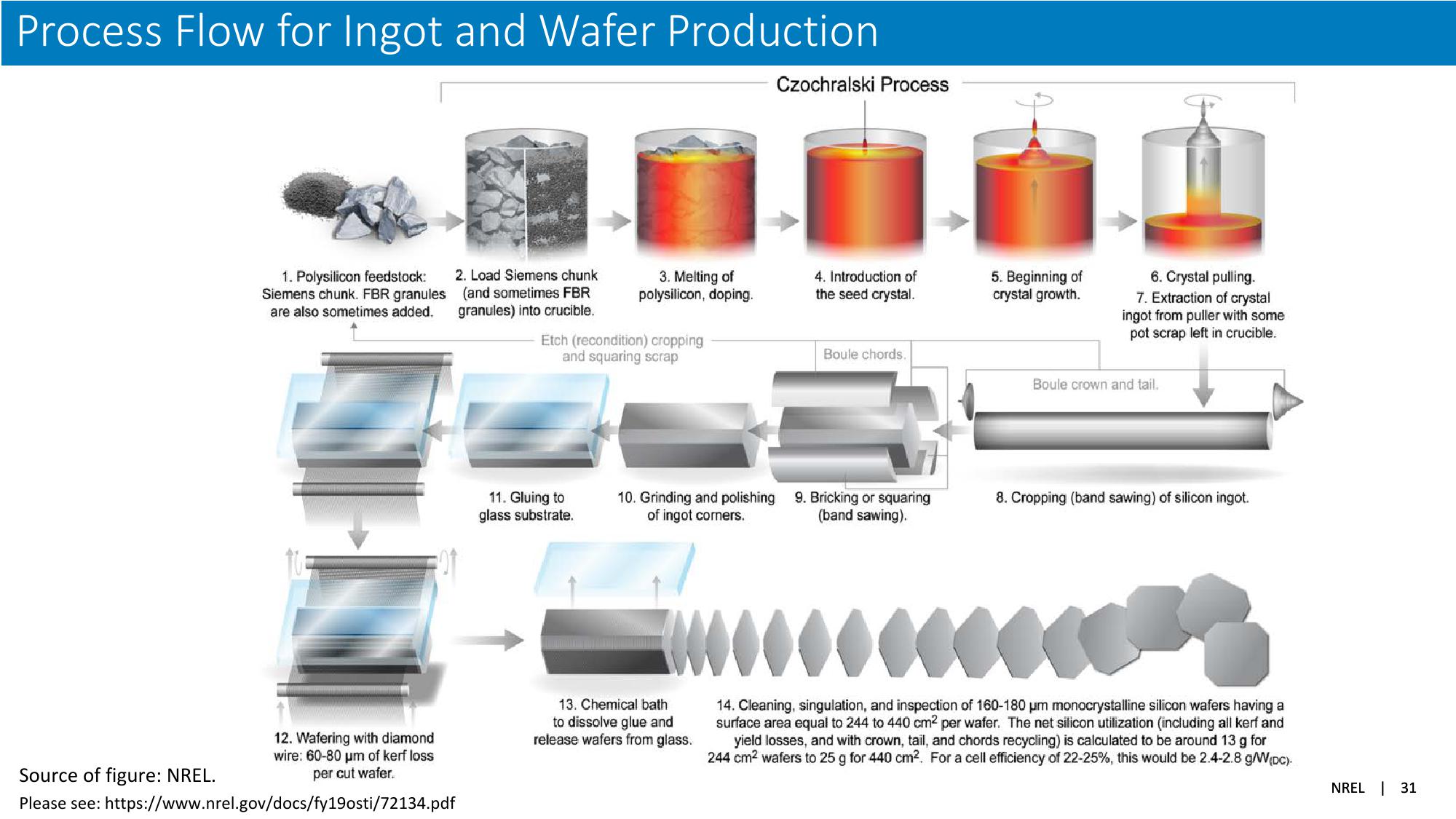
Process Flow for Ingot and Wafer Production
Czochralski Process
1. Polysilicon feedstock:
Siemens chunk. FBR granules
are also sometimes added.
2. Load Siemens chunk
(and sometimes FBR
granules) into crucible.
3. Melting of
polysilicon, doping.
Etch (recondition) cropping
and squaring scrap
10:
12. Wafering with diamond
Source of figure: NREL.
wire: 60-80 μm of kerf loss
per cut wafer.
Please see: https://www.nrel.gov/docs/fy19osti/72134.pdf
4. Introduction of
the seed crystal.
5. Beginning of
crystal growth.
6. Crystal pulling.
7. Extraction of crystal
ingot from puller with some
pot scrap left in crucible.
Boule chords.
Boule crown and tail.
11. Gluing to
glass substrate.
10. Grinding and polishing 9. Bricking or squaring
of ingot corners.
(band sawing).
8. Cropping (band sawing) of silicon ingot.
13. Chemical bath
to dissolve glue and
release wafers from glass.
14. Cleaning, singulation, and inspection of 160-180 μm monocrystalline silicon wafers having a
surface area equal to 244 to 440 cm2 per wafer. The net silicon utilization (including all kerf and
yield losses, and with crown, tail, and chords recycling) is calculated to be around 13 g for
244 cm² wafers to 25 g for 440 cm². For a cell efficiency of 22-25%, this would be 2.4-2.8 g/W(pc).
NREL 31View entire presentation