The Global Solar Photovoltaic Supply Chain and Bottom-UP Cost Model Results
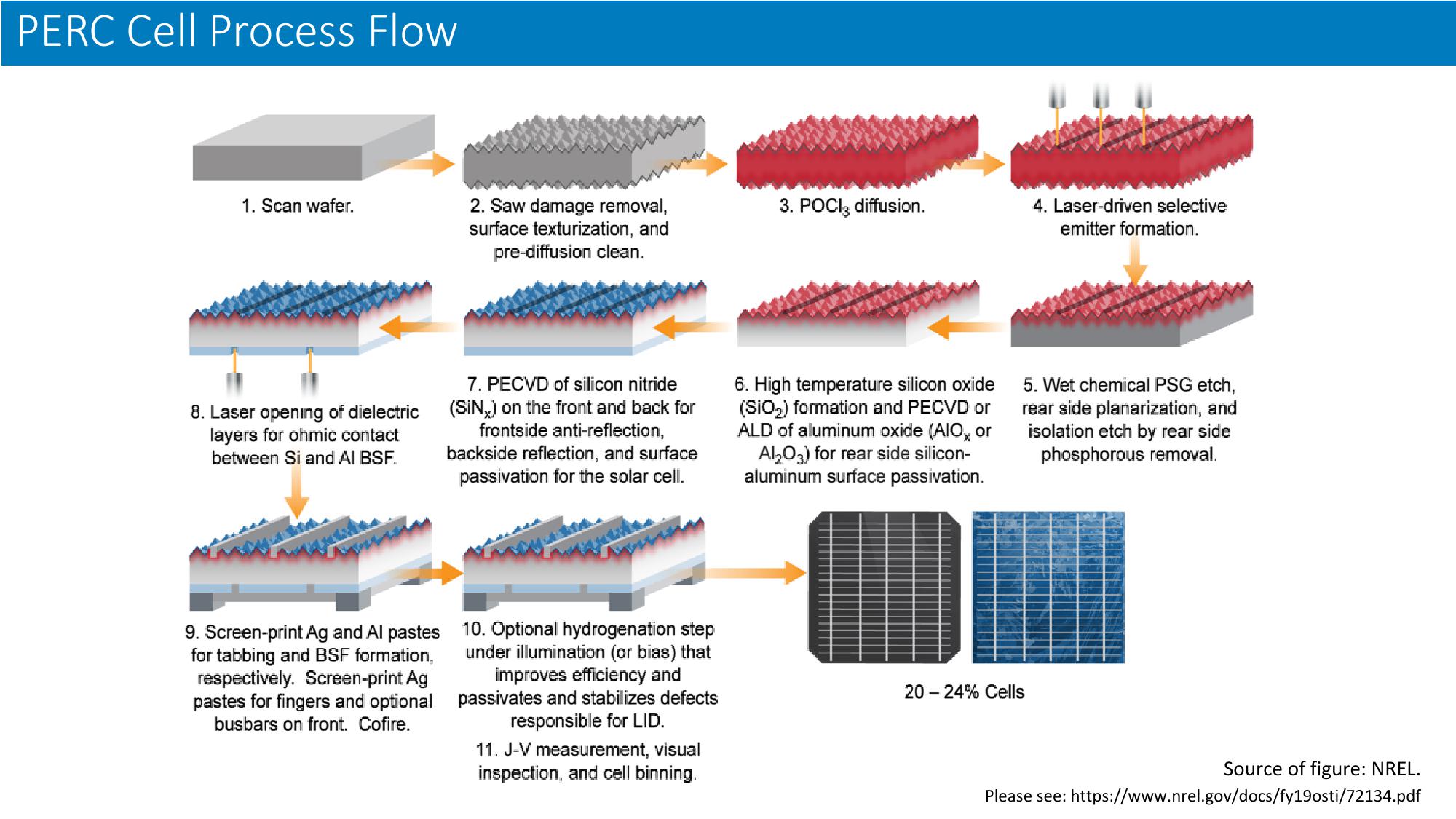
PERC Cell Process Flow
1. Scan wafer.
2. Saw damage removal,
surface texturization, and
pre-diffusion clean.
3. POCI3 diffusion.
4. Laser-driven selective
emitter formation.
8. Laser opening of dielectric
layers for ohmic contact
between Si and AI BSF.
7. PECVD of silicon nitride
(SiNX) on the front and back for
frontside anti-reflection,
backside reflection, and surface
passivation for the solar cell.
6. High temperature silicon oxide
(SiO2) formation and PECVD or
ALD of aluminum oxide (AIO* or
Al2O3) for rear side silicon-
aluminum surface passivation.
5. Wet chemical PSG etch,
rear side planarization, and
isolation etch by rear side
phosphorous removal.
9. Screen-print Ag and Al pastes
for tabbing and BSF formation,
respectively. Screen-print Ag
pastes for fingers and optional
busbars on front. Cofire.
10. Optional hydrogenation step
under illumination (or bias) that
improves efficiency and
passivates and stabilizes defects
responsible for LID.
11. J-V measurement, visual
inspection, and cell binning.
20-24% Cells
Source of figure: NREL.
Please see: https://www.nrel.gov/docs/fy19osti/72134.pdfView entire presentation