KLA Investor Day Presentation Deck
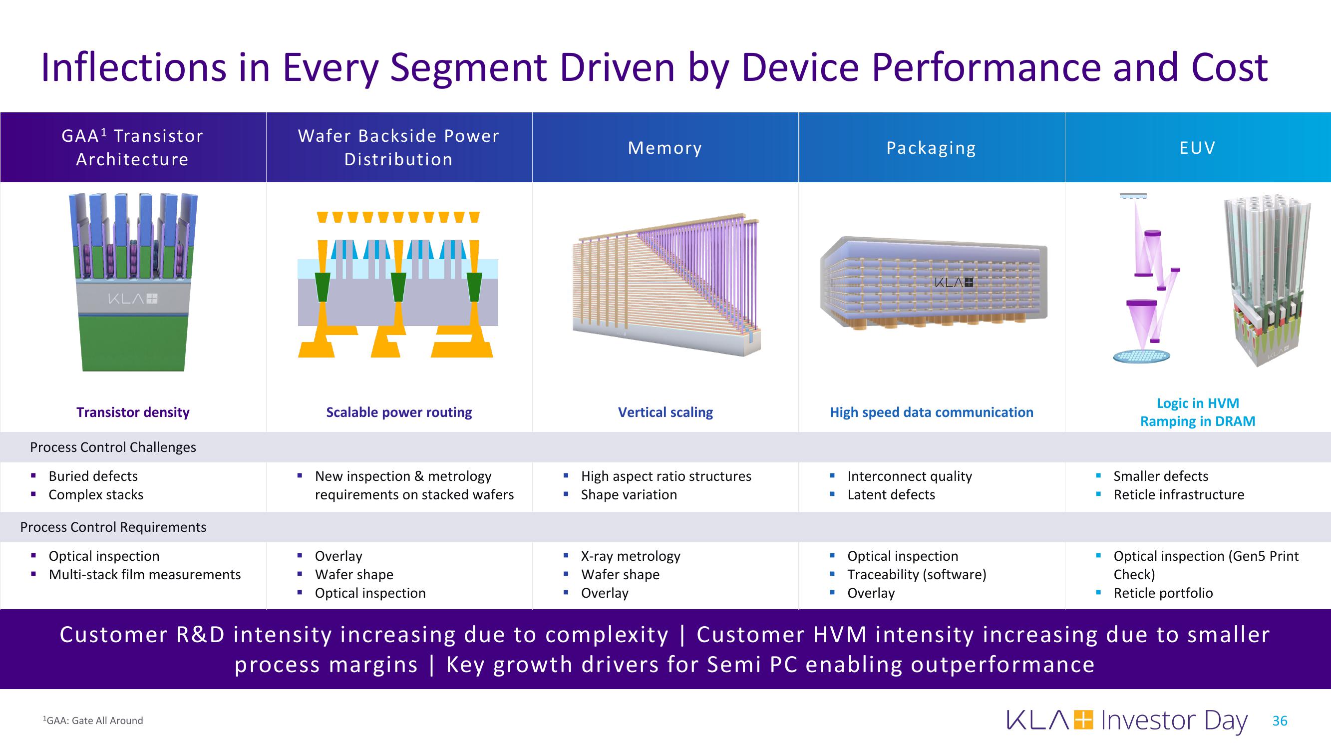
Inflections in Every Segment Driven by Device Performance and Cost
GAA¹ Transistor
Architecture
Wafer Backside Power
Distribution
H
KLA#
Transistor density
Process Control Challenges
I
■ Buried defects
▪ Complex stacks
Process Control Requirements
Optical inspection
Multi-stack film measurements
ZANIA
N
¹GAA: Gate All Around
Scalable power routing
New inspection & metrology
requirements on stacked wafers
I Overlay
■ Wafer shape
▪ Optical inspection
H
Memory
Vertical scaling
High aspect ratio structures
Shape variation
▪ X-ray metrology
▪ Wafer shape
Overlay
High speed data communication
I Interconnect quality
Latent defects
■
Packaging
I Optical inspection
■
■
Traceability (software)
Overlay
■
■
EUV
Logic in HVM
Ramping in DRAM
Smaller defects
Reticle infrastructure
KLAB
Optical inspection (Gen5 Print
Check)
Reticle portfolio
Customer R&D intensity increasing due to complexity | Customer HVM intensity increasing due to smaller
process margins | Key growth drivers for Semi PC enabling outperformance
KLAH Investor Day 36View entire presentation