KLA Investor Day Presentation Deck
Case Study: SPTS Plasma Dicing for Advanced Packaging
Wafers are cut into single
die in a singulation process
before final assembly
■
■
■
Problem
Wafer singulation is usually done with blade and/or
laser, which creates particles and cracks
Defects can lead to failures of entire multi-die
package, causing huge economic losses
Plasma etch based singulation provides superior
cleanliness, but integration is complex
Solution
Developed differentiated plasma dicing solution
State-of-the-art demo lab created to develop full
integration process around wafer singulation
Validated process performance via multiple
advanced customer collaborations
SPTS
Mass
SPTS Mosaic plasma dicing
TM
$M
CY16
Results
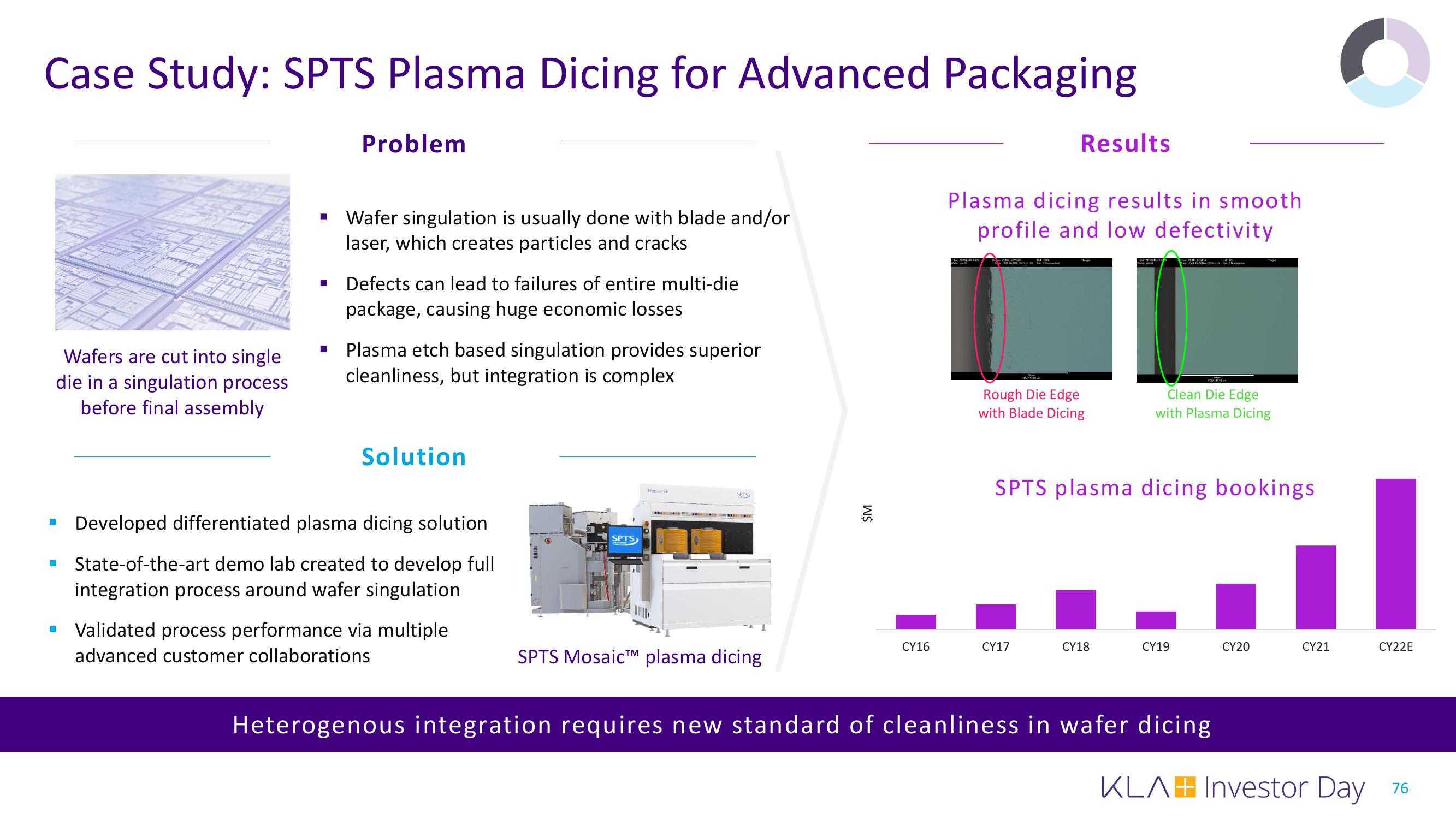
Plasma dicing results in smooth
profile and low defectivity
Rough Die Edge
with Blade Dicing
CY17
SPTS plasma dicing bookings
CY18
PM FLACHADIGING D
Clean Die Edge
with Plasma Dicing
CY19
Heterogenous integration requires new standard of cleanliness in wafer dicing
CY20
CY21
CY22E
KLAH Investor Day 76View entire presentation